
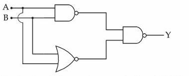
For the circuit shown above, the equivalent gate is:
- A
AND gate
- B
OR gate
- C
NAND gate
- D
NOT gate
For the circuit shown above, the equivalent gate is:
AND gate
OR gate
NAND gate
NOT gate
Correct answer:D
Standard Method
Given: A logic circuit with inputs and .
Find: The equivalent gate of the complete circuit.
From the circuit, the top gate is a NAND gate taking inputs and . Its output is
The bottom gate is a NOR gate taking inputs and . Its output is
These two outputs are applied to the final NAND gate. Therefore,
Now use De Morgan's law:
and
Substituting,
Using absorption,
Hence,
Again by De Morgan's law,
Therefore, the given circuit is equivalent to an OR gate. The solution contains contradictory text, but its final declared answer is inconsistent with the actual circuit diagram. The correct equivalent gate from the circuit is OR gate, so the most defensible option is B.
Mistake: Treating the lower gate as an OR gate followed by a NOT gate separately from the drawn symbol. Why wrong: the symbol shown is already a NOR gate. What to do instead: identify each gate directly from its symbol before writing Boolean expressions.
Mistake: Using the text of the solution without checking it against the circuit diagram. Why wrong: the written explanation contradicts the actual connections and gate symbols. What to do instead: derive the Boolean expression from the diagram itself and then simplify.
Mistake: Forgetting that the final gate is a NAND gate, not an AND gate. Why wrong: missing the output bubble changes the final complement and gives a wrong equivalent expression. What to do instead: always account for inversion bubbles at gate outputs.
Get unlimited AI-adaptive practice, mastery tracking, and an AI tutor that explains every step — free to start.