MCQMediumJEE Main 2026 · 22 January, Shift 2Logic Gates

Physics Question from JEE Main 2026 · 22 January, Shift 2

The correct truth table for the given input data of the following logic gate is:
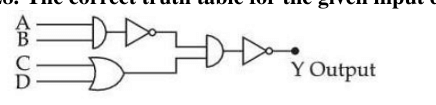
Logic circuit with inputs A and B entering an AND gate followed by a NOT gate, inputs C and D entering an OR gate, both outputs feeding an AND gate followed by a NOT gate to produce Y output.
  • A

    ABCDY11011001101010011111\begin{array}{|c|c|c|c|c|}\hline A & B & C & D & Y \\ \hline 1 & 1 & 0 & 1 & 1 \\ 0 & 0 & 1 & 1 & 0 \\ 1 & 0 & 1 & 0 & 0 \\ 1 & 1 & 1 & 1 & 1 \\ \hline \end{array}

  • B

    ABCDY11011001101010111110\begin{array}{|c|c|c|c|c|}\hline A & B & C & D & Y \\ \hline 1 & 1 & 0 & 1 & 1 \\ 0 & 0 & 1 & 1 & 0 \\ 1 & 0 & 1 & 0 & 1 \\ 1 & 1 & 1 & 1 & 0 \\ \hline \end{array}

  • C

    ABCDY11010001101010111111\begin{array}{|c|c|c|c|c|}\hline A & B & C & D & Y \\ \hline 1 & 1 & 0 & 1 & 0 \\ 0 & 0 & 1 & 1 & 0 \\ 1 & 0 & 1 & 0 & 1 \\ 1 & 1 & 1 & 1 & 1 \\ \hline \end{array}

  • D

    ABCDY11010001111010111111\begin{array}{|c|c|c|c|c|}\hline A & B & C & D & Y \\ \hline 1 & 1 & 0 & 1 & 0 \\ 0 & 0 & 1 & 1 & 1 \\ 1 & 0 & 1 & 0 & 1 \\ 1 & 1 & 1 & 1 & 1 \\ \hline \end{array}

Answer & step-by-step solution

Sign in to reveal the correct answer, the full step-by-step solution, and the common mistakes for this question.

Practice more Logic Gates questions

Get unlimited AI-adaptive practice, mastery tracking, and an AI tutor that explains every step - free to start.

Related questions