MCQEasyJEE 2023Logic Gates

JEE Physics 2023 Question with Solution

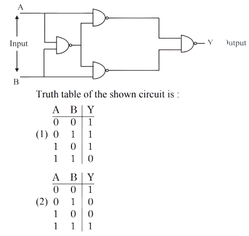
The output YY for the inputs AA and BB of the circuit is given by:

Logic gate circuit with inputs A and B feeding a network of NAND gates and final output Y.Four truth table options for inputs A, B and output Y corresponding to the shown logic circuit.
  • A

    ABY001011101110\begin{array}{c|c|c}A & B & Y \\ \hline 0 & 0 & 1 \\ 0 & 1 & 1 \\ 1 & 0 & 1 \\ 1 & 1 & 0\end{array}

  • B

    ABY001010100111\begin{array}{c|c|c}A & B & Y \\ \hline 0 & 0 & 1 \\ 0 & 1 & 0 \\ 1 & 0 & 0 \\ 1 & 1 & 1\end{array}

  • C

    ABY000011101111\begin{array}{c|c|c}A & B & Y \\ \hline 0 & 0 & 0 \\ 0 & 1 & 1 \\ 1 & 0 & 1 \\ 1 & 1 & 1\end{array}

  • D

    ABY000011101110\begin{array}{c|c|c}A & B & Y \\ \hline 0 & 0 & 0 \\ 0 & 1 & 1 \\ 1 & 0 & 1 \\ 1 & 1 & 0\end{array}

Answer

Correct answer:D

Step-by-step solution

Standard Method

Given: The logic circuit has inputs AA and BB. Find: The correct truth table for output YY.

Given circuit represent XOR.

The circuit is an implementation of the XOR gate using NAND gates. Therefore its output is

Y=ABY = A \oplus B

The XOR truth table is

ABY000011101110\begin{array}{c|c|c} A & B & Y \\ \hline 0 & 0 & 0 \\ 0 & 1 & 1 \\ 1 & 0 & 1 \\ 1 & 1 & 0 \end{array}

Therefore, the correct option is D.

Truth Table Verification

Given: The circuit is made of NAND gates. Find: Which option matches the output YY.

To solve the given circuit and determine the output YY for the inputs AA and BB, analyze the logic gates used in the circuit.

The circuit provided in the image represents an XOR gate. The intermediate outputs are:

AB\overline{A \cdot B}

The next two NAND gate outputs become

AAB\overline{A \cdot \overline{A \cdot B}}

and

BAB\overline{B \cdot \overline{A \cdot B}}

The final NAND gate gives

Y=(AABBAB)Y = \overline{\left(\overline{A \cdot \overline{A \cdot B}} \cdot \overline{B \cdot \overline{A \cdot B}}\right)}

Evaluating for all input combinations:

  1. When A=0A = 0 and B=0B = 0, Y=0Y = 0.
  2. When A=0A = 0 and B=1B = 1, Y=1Y = 1.
  3. When A=1A = 1 and B=0B = 0, Y=1Y = 1.
  4. When A=1A = 1 and B=1B = 1, Y=0Y = 0.

So the truth table is

ABY000011101110\begin{array}{c|c|c} A & B & Y \\ \hline 0 & 0 & 0 \\ 0 & 1 & 1 \\ 1 & 0 & 1 \\ 1 & 1 & 0 \end{array}

Hence, the given circuit represents an XOR gate and the correct option is D.

Truth table showing inputs A and B with output Y equal to 0, 1, 1, 0 for the four combinations.

Common mistakes

  • Mistake: Treating the network as a single NAND gate output. Why it is wrong: the combination of several NAND gates changes the logic function. What to do instead: identify the full gate combination before writing the truth table.

  • Mistake: Confusing XOR with XNOR. Why it is wrong: XOR gives output 11 when the inputs are different, while XNOR gives output 11 when the inputs are the same. What to do instead: check the rows (0,1)(0,1) and (1,0)(1,0) carefully.

  • Mistake: Reading option numbering incorrectly and mapping Option 4 to the wrong label. Why it is wrong: in the final record, the fourth option corresponds to label D. What to do instead: map options in order as A, B, C, D.

Practice more Logic Gates questions

Get unlimited AI-adaptive practice, mastery tracking, and an AI tutor that explains every step — free to start.

Related questions