
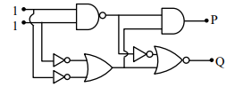
In the digital circuit shown in the figure, for the given inputs the and values are:
- A
- B
- C
- D
Option text unavailable
In the digital circuit shown in the figure, for the given inputs the and values are:
Option text unavailable
Correct answer:B
Standard Method
Given: The digital logic circuit has both inputs equal to .
Find: The values of and .
From the solution, the gate operations are evaluated step by step.
The top-left gate is a NAND gate with inputs and . Therefore,
and hence,
This output is sent to the lower-left OR section and also to the rightmost AND gate.
The lower-left OR gate receives inputs and . So,
This then passes through a NOT gate, giving
The NOR gate for receives inputs and . Therefore,
and so,
For , the rightmost AND gate receives inputs and . Thus,
Therefore, the outputs are and .
The solution explicitly concludes that the correct option is B and also states . Since the listed options are shifted in the provided input, the value-based correct answer corresponds to the first available option text.
Gate-by-Gate Evaluation
Given: Both inputs are HIGH, i.e. and .
Find: Output values of and .
so
Hence . 5. For the top-right AND gate:
Hence .
So the final output is .
Treating the first gate as an AND gate instead of a NAND gate is incorrect because the output bubble means inversion. First compute AND, then complement the result.
Ignoring the inverter after the OR gate gives the wrong input to the NOR gate. The OR output must be inverted before it enters the final gate.
Confusing the final NOR gate with an OR gate is wrong because the output bubble changes OR into NOR. Compute OR first, then take its complement.
Get unlimited AI-adaptive practice, mastery tracking, and an AI tutor that explains every step — free to start.