
Match the List I with List II:
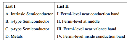

Choose the correct answer from the options given below:
- A
(A) I, (B) II, (C) III, (D) IV
- B
(A) II, (B) I, (C) III, (D) IV
- C
(A) II, (B) III, (C) I, (D) IV
- D
(A) III, (B) I, (C) II, (D) IV
Match the List I with List II:
Choose the correct answer from the options given below:
(A) I, (B) II, (C) III, (D) IV
(A) II, (B) I, (C) III, (D) IV
(A) II, (B) III, (C) I, (D) IV
(A) III, (B) I, (C) II, (D) IV
Correct answer:D
Standard Method
Given: Match semiconductor types and metals with the correct position of the Fermi-level.
Find: The correct option.
For an intrinsic semiconductor, the Fermi-level lies at the middle of the valence and conduction bands, so A II.
For an n-type semiconductor, the Fermi-level lies near the conduction band, so B I.
For a p-type semiconductor, the Fermi-level lies near the valence band, so C III.
For metals, the Fermi-level lies inside the conduction band, so D IV.
Thus the matching is:
Therefore, the correct option is D.
Placing the Fermi-level of an intrinsic semiconductor near one band is wrong because in a pure semiconductor it lies approximately at the middle of the band gap. Match intrinsic semiconductor with II.
Confusing n-type and p-type semiconductors is a common error. In n-type, electrons are majority carriers so the Fermi-level shifts toward the conduction band; in p-type, it shifts toward the valence band.
Assuming metals have a band gap like semiconductors is incorrect. In metals, the Fermi-level lies inside the conduction band, so it must be matched with IV.
Get unlimited AI-adaptive practice, mastery tracking, and an AI tutor that explains every step — free to start.